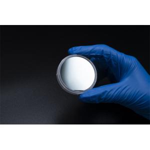
2inch Green-LED GaN on silicon wafer
Overview
Gallium nitride (GaN) is creating an innovative shift throughout the power electronics world. For decades, silicon-based MOSFETs (Metal Oxide Semiconductor Field Effect Transistors) have been an integral part of the everyday modern world that helps convert energy to power.
Generative adversarial networks (GANs) are algorithmic architectures that use two neural networks, pitting one against the other (thus the “adversarial”) in order to generate new, synthetic instances of data that can pass for real data. They are used widely in image generation, video generation and voice generation.
| 2-4inch Green-LED GaN on silicon |
| Item Si(111) substrates |
Al(Ga)N buffer |
uGaN |
nGaN |
MQW(1-3 pairs) |
AlGaN |
pGaN |
Contact layer |
| InGaN-QW |
GaN-QB |
| Dimensions |
2 inch,4 inch |
| |
520±10nm |
| Thickness |
800nm |
1000nm |
3000nm |
~3nm |
~10nm |
35nm |
145nm |
20nm |
| Composition |
Al% |
/ |
/ |
/ |
/ |
/ |
~15 |
/ |
/ |
| In% |
/ |
/ |
/ |
~25 |
/ |
/ |
/ |
/ |
| Doping |
[Si] |
/ |
/ |
8.0E+18 |
/ |
2.0E+17 |
/ |
/ |
/ |
| [Mg] |
/ |
/ |
/ |
/ |
/ |
1.0E+20 |
3.0E+19 |
2.0E+20 |
| Substrate Structure |
20nmContact layer/145nmpGaN/35nmAlGaN/~10nmGaN-QB/~3Si(111)substrates |
| Package |
Packaged in a class 100 clean room environment, in 25PCS container, under a nitrogen atmosphere |
About Us
We specialize in processing a variety of materials into wafers, substrates and customized optical glass parts.components widely used in electronics, optics, opto electronics and many other fields. We also have been working closely with many domestic and oversea universities, research institutions and companies, provide customized products and services for their R&D projects. It's our vision to maintaining a good relationship of cooperation with our all customers by our good reputations.
FAQ
Q: Are you trading company or manufacturer ?
We are factory.
Q: How long is your delivery time?
Generally it is 3-5 days if the goods are in stock.
or it is 7-10 days if the goods are not in stock, it is according to quantity.
Q: Do you provide samples ? is it free or extra ?
Yes, we could offer the sample for free charge but do not pay the cost of freight.
Q: What is your terms of payment ?
Payment <=5000USD, 100% in advance.
Paymen >=5000USD, 80% T/T in advance , balance before shippment.